Circuit Description

Click on the diagram above to get a larger PDF version, which allows you to see more details.
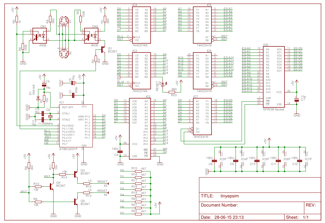
The diagram is part of the download package. You'll find the 32kB RAM chip of the type 62256 in the center of the circuit. I recommend you use a cache RAM chip that can be salvaged from an old obsolete 80386 or 80486 board. These chips are not only very cheap, they are also very fast. As a bonus they even have a smaller foot print than a normal 62256.
This RAM chip must be accessible by the target system and by the internal micro controller. Obviously this can never be allowed to happen simultaneously. The internal controller is allowed access to the RAM chip when the target system is held in RESET. When RESET is released the target system is allowed access to the RAM chip. That way the two systems are in no danger of interfering with each other.
 The 3 buffers 74HC541 are used to isolate the target system from the RAM chip.
Two of them are used to connect the 15 address lines from the target system to the address lines of the RAM chip.
Under program control these 15 address lines can be switched to tri-state, effectively disconnecting the target system.
The 3rd buffer IC is connected the other way around and takes care of delivering the 8 data lines to the target system.
The two output enable signals of this IC are connected to the OE and CE lines of the target system's EPROM socket.
This way the Tiny EPROM Simulator will operate in exactly the same way as a normal EPROM would.
Two latches of the type 74HC574 take care of holding up to 15 address lines generated by the micro controller.
These latches serve two purposes: hold the address that is to be written to and isolate the micro controller from the RAM when the target system is running.
Only 15 address lines are needed, leaving one spare bit on the latches.
This bit is used to connect an LED which indicates when the target system is held in RESET by the Tiny EPROM Simulator.
The data lines of the RAM are directly connected to 8 I/O lines of the micro controller.
These lines also take care of loading the two latches.
When the target system is running these 8 lines are held high, effectively making them inputs that don't interfere with the rest of the system.
The I/O pins on the micro controller's P3 are used to communicate with the SB-Bus and control the latches and address buffers.
P3.0 is used as a serial input, while P3.1 is used as serial output.
P3.2 and P3.3 control the clock signals for the two latches.
A low pulse on such a line freezes the contents of the inputs to the outputs.
P3.4 is used to select between RAM access by the micro controller (H), or target system (L).
This same signal is also used to drive the two RESET transistors, one for each polarity.
P3.5 controls the write input to the RAM chip.
It is held high when the target system is accessing the RAM.
P3.7 is used to control the OE signal of the RAM chip.
This signal is held low during target system operation.
It is held high when the target system is held in RESET to avoid collisions between data coming from the micro controller and data coming from the RAM chip.
Naturally the micro controller needs a crystal oscillator and a Reset circuit. But my guess is that this doesn't need any further explanation.
The SB-Bus interface completes the circuit description.
Two opto-couplers are the main ingredients.
They isolate the SB-Bus from all other devices.
The output of the micro controller can pull the base of the PNP transistor low, which makes it conduct, which makes the opto-coupler to start conducting as well.
The receiving opto-coupler can pull the input of the micro controller low.
Normally this input is held high by a 1kΩ resistor.
The two 100kΩ resistors speed up the transitions of the opto-couplers, making the ramps somewhat steeper.
Bill Of Materials
| Part | Qtty | Description |
| AT89C2051 | 1 | Programmed with software |
| 74HC574 | 2 | LS or HCT should work too |
| 74HC541 | 3 | LS or HCT should work too |
| 62256 | 1 | Tip: Use cache RAM from an old 386 board |
| 4N35 | 2 | Opto-coupler |
| Resistor 10Ω | 2 | |
| Resistor 390Ω | 2 | |
| Resistor 1kΩ | 1 | |
| Resistor 2k2 | 2 | |
| Resistor 4k7Ω | 8 | |
| Resistor 680Ω | 1 | |
| Resistor 10kΩ | 5 | |
| Resistor 100kΩ | 2 | |
| Capacitor 100µF/10V | 1 | |
| Capacitor 10µF/10V | 2 | |
| Capacitor 100nF | 7 | |
| Capacitor 18pF | 2 | |
| Diode 1N4148 | 1 | Or any other universal switching diode |
| Transistor BC547 | 2 | Or any other universal NPN transistor |
| Transistor BC557 | 2 | Or any other universal PNP transistor |
| LED | 1 | Any colour and size you like |
| Crystal 11.0592MHz | 1 | |
| 4 way mini-DIN connector | 2 | |
| 28 way DIL plug | 1 | |
| 34 way header with connector | 1 | To be used at other end of flat cable |
| 28 way flat cable | 1 | About 15cm long |
| mini connector | 2 | One red, one black for RESET outputs |
| 20 way IC socket | 6 | |
| 28 way IC socket | 2 | |
