The Hardware Part 2
The Display
Let's start this page with the description of the display.
Starting there will help you to better appreciate the rest of the circuit too.
I've decided to use a multipexed display, not because it was absolutely necessary.
But because I had 2 good reasons for it, at first.
The first good reason was that I had only one BCD to 7-segment decoder IC in my junk box and I didn't want to get out and buy 3 extra.
This alone is a very good reason to have a multiplexed display, if you ask me.
After all I wanted to build this clock with parts which I had in stock, period.
The second reason was that a multiplexed display would only require 12 wires to connect between the main PCB and the display PCB.
A non multiplexed display would require a total of 36 wires.
Later I decided to mount the displays directly on the main PCB though, so this advantage is no longer valid.
At least not for my clock.
Of course you may decide otherwise if you want to build this clock yourself.
There's not much difference in the component count between a multiplexed and a non multiplexed display either.
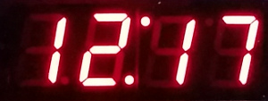 The display consists of a total of 4 digits, grouped together in two parts.
They are common Anode displays.
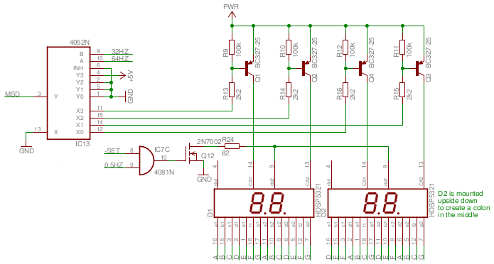
And as you can read from the diagram the minutes display is actually mounted upside down on the front panel PCB.
That way the two adjacent display's decimal points will form a colon.
The digits themselves are symmetrical, so you won't be able to see any difference there.
The anodes of the 4 digits are driven by 4 transistors Q1 to Q4.
These transistors are driven by the outputs of IC13 a 1-4 multiplexer/demultiplexer.
I've tied the input of this demultiplexer to ground, and only one of the 4 transistors will receive a base current at any given time.
Which transistor is selected depends on the 2-bit input signal on pins A and B of IC13.
These signals are derived from the time-base and all 4 states have exactly the same duration.
The 128Hz signal ensures that the display is scanned fast enough, so we won't be able to see that the display is multiplexed.
IC7C drives a FET, which controls the center two decimal points, which form the colon between the minutes and hours displays.
When the clock is in RUN mode this colon will flash at a rate of 0.5Hz, so the colon will be on for one second, and off the next, repeatedly.
In SET mode the colon is switched off completely, indicating that the clock is no longer running.
There'se one thing in this diagram which may not be very obvious right now. It's the second half of IC13, the MSD output on pin 3. This signal is high when the Most Significant Digit is switched on. This in turn is used to blank the most significant digit when it's 0 later on.
The Segment Drivers
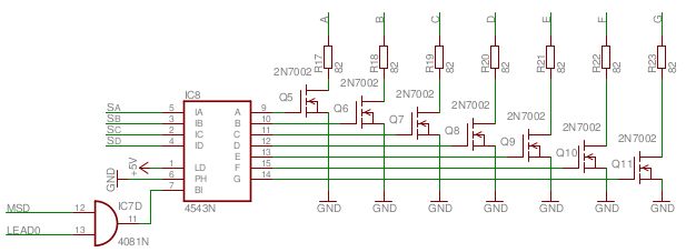
The displays are multiplexed, therefore we only need just one BCD to 7-segment decoder. Unfortunately the 4543 can only drive 10mA per output, just enough for a non multiplexed LED. Not to worry, I simply add 7 MOS-FETs to the design to amplify the drive capacity. The series resistors limit the LED current to some 40mA, which is a nice 10mA average when shared by 4 digits.
IC7D combines the MSD and LEAD0 signals together and this signal will blank the display when the hours counter is below 10, effectively suppressing the leading 0.
We're not interested in the latching feature of the display driver, and therefore the LD pin is tied to the positive supply rails. The phase of the output is inverted by the MOS-FETs, and that's why the PH input is tied to ground.
The Multiplexer
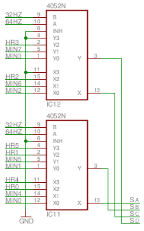
The multiplexer completes the display part of the clock. Its purpose is to sequencially scan through all 4 digits of the hours and minutes counters.
We need to multiplex 4 bits from 4 digits.
That's why we have four 1-4 multiplexers/demultiplexers, packed in two ICs.
There's always just one of the 4 inputs connected to the output of these 4 multiplexers.
The A and B inputs determine which one of the 4 inputs gets connected to the output.
The displays are scanned at 128Hz, which is well above the maximum visible frequency of the human eye.
Why 128Hz?
Because it was available on the time base prescaler, together with the 64Hz signal.
Together they form a 2 bit multiplexer selection signal.
The Power Supply
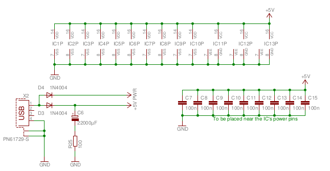
The only part of the schematic which we haven't discussed yet is the power supply.
CMOS circuits draw very little power.
And on top of that the power they need doesn't have to be regulated either.
They are happy with anything between some 3V and 15V.
I run the clock from a 5V mobile phone charger.
That way I don't have to worry about the high voltage stuff, the rectifying and filtering, the generated heat and the required space, which normally are involved in a power supply.
This has only one little disadvantage though.
We can't use the mains frequency as a relatively accurate time base anymore.
But we've already taken care of that part with a watch crystal.
The input voltage is fed to almost the entire circuit through one series diode D3.
That way we can use a gold cap C6 to provide power for a while in case the mains power is failing.
Thus the clock will continue running for about an hour without mains power.
Only the displays are supplied with the power coming directly from the input.
It goes without saying that the power hungry LED displays can not be supplied by the gold cap for very long, thus the displays will go dark when the power is removed.
You may be wondering what D4 doing there, in series with the power supply to the displays.
No it's not for reverse polarity protection, as the chances for that to happen are neglectable.
If this diode was missing, the emitter voltage of the anode driver transistors would be 5V.
The base voltage of these transistors cannot be higher than the supply voltage of the logic, which is 4.4V because of the voltage drop over D3.
Therefore the transistors will probably not be switched off completely, producing ghost segments on the display.
With D4 in place the emitter voltage of the driver transistors is lowered to 4.4V too, avoiding this potential problem.
R25 will limit the inrush current to the gold cap when it is empty. The total logic circuit draws only 32µA, which will produce a voltage drop of just 3.2mV over R25 when the main power is removed. This 3.2mV is neglectable and will have no influence on the operation of the circuit.
How long the clock can run without mains power depends on several things. I have no idea how much tolerance there is in power consumption of the different CMOS components from varying manufacturers. My clock can run for more than an hour without input power. I didn't bother to find out how much longer, I was quite satisfied with reaching one whole hour.
It goes without saying that the bypass caps C7 to C15 are to be placed as close to the power supply pins of the ICs on the circuit board. There are only 9 bypass caps for 13 ICs, so some ICs can share one bypass cap. For instance each of the counters can share a cap with the adjacent NAND or AND gate ICs.
There's one thing missing in this power supply.
You will be looking for a fuse in vain.
Mobile phone power supplies are current limited anyway.
And what could go wrong if you did have a short circuit somewhere in this clock?
Absolutely nothing.
So I didn't bother putting a fuse in.
Feel free to use a fuse yourself if you're not comfortable with that idea.
A 315mA fuse would be adequate.
