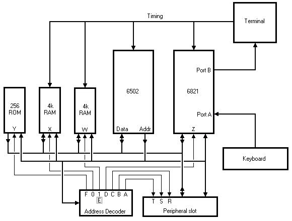
Apple 1 Block Diagram

Here it is, the entire Apple 1 overview. Not much of a computer by today's standards, but sure enough it was a reasonably sized computer back then. In fact it had more memory than the computer in the Apollo 11, which landed the first men on the moon some 6 years before.
At the heart of the diagram we see the 6502, Apple 1's microprocessor.
All timing is derived from the terminal circuitry.
And that's where the processor's 1MHz clock signal originates from too.
The memory consists of 2 banks of 4k dynamic RAM and one tiny ROM with only 256 bytes, occupying an entire 4k bank.
The dynamic memory is refreshed by "stealing" some clock cycles away from the processor.
Explaining how this is done is a bit beyond the purpose of this page.
Finally the "computer" part is completed by a PIA (Peripheral I/O Adapter), responsible for keyboard input and terminal output.
The keyboard is simply a standard ASCII keyboard.
It produced a 7-bit ASCII character whenever a key was pressed.
A key press is signalled by a short strobe pulse, which sets a flip-flop inside the PIA to trigger the software to read the new character from the keyboard.
The terminal is simply a character output device which will be described on a separate page.
 All computer parts are glued together by the address decoder.
This decoder splits the 64k address range into 16 equal banks of 4kB each.
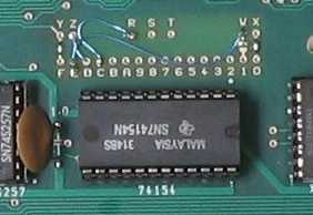
Steve provided for a little patching area to allow you to flexibly arrange the memory in a way which suits you best.
There are 2 mandatory address banks: Bank 0, which must hold RAM memory for page 0 and the system stack.
And Bank F which must hold ROM memory to boot from.
You can see in the picture here that a simple blob of solder can be used to bridge the gaps between 0 and X and between Y and F to achieve just that.
In this picture the bridge between 1 and W is not shorted by a blob of solder, instead a wire is used to connect block 1 of RAM memory to bank E to accommodate the Apple Basic interpreter read from tape.
But if you want to you can connect block 1 of RAM to bank 1 in memory, creating a total of 8k of continuous RAM space.
Finally you see a very common patch between R and C, which is in fact the block of memory used by the cassette interface in the peripheral slot.
Usually S is patched to B, and T is patched to A too for expansion purposes although I have never seen any "official" use for them.
The signals R, S and T are connected to the peripheral connector, which usually is filled with the ACI, the Apple Cassette Interface.
Not shown in the block diagram is the expansion connector. The expansion connector is an edge connector on the right side of the Apple 1 which can be used to expand the system with more RAM and I/O. This connector is simply a collection of just about all data, address and relevant timing signals.
