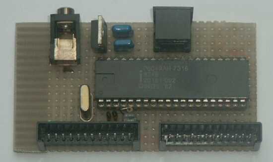
8049 Spy

What do you do when you have to read the internal ROM contents of a 8048 or 8049 processor and you don't own a programmer for those devices?
You simply build this 8049 spy of course!
That is exactly what I did when I wanted to know how my Philips Frequency Counter PM 6668 worked.
With this knowledge I was able to add some interesting features to that beautiful old counter.
You can find a description of the SB-6668 project elsewhere on this site.
This 8049 Spy is not a stand alone project.
It is designed as an I/O expansion to my 6802 Nano Computer.
So if you're interested in this 8049 Spy, you should start building the 6802 Nano Computer first.
As an alternative you can connect the 8049 Spy to just about any other micro controller that has about 12 I/O lines free (or 11 and one serial output).
But then you'll have to write the program that reads the ROM contents yourself, something that is not that difficult really.
Operation of the 8049 Spy is not difficult.
Simply insert the 8048 or 8049 processor you want to read, apply the 12V power supply and the contents of the ROM will be transferred through the serial link to your PC.
The file is transferred in Intel Hex format, and the communication is set to 9600 baud, 8 data bits, no parity, 1 stop bit.
A total of 4kB is transferred this way.
Originally the 8048 only has 1kB of ROM, and the 8049 contains 2kB of ROM.
But since the addressing mechanism of the 8048 family was designed to accommodate a maximum of 4kB, I decided to read the entire 4kB address space to be future prepared.
You can simply ignore or delete the part of the file that you're not interested in.
Circuit Description
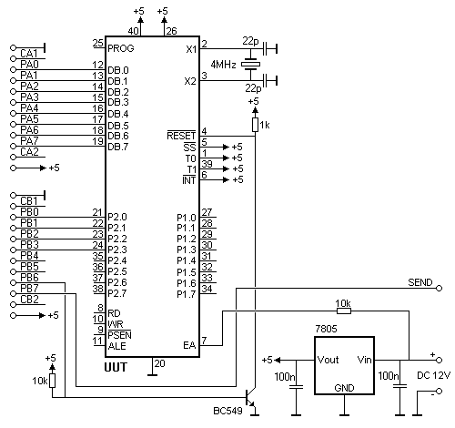
 As you can see in this diagram you don't need too much hardware to read the ROM contents of an 8049.
The main part in the diagram is the 8049 (or 8048) that you want to read.
Apart from that you only need a voltage regulator, an inverter circuit and a crystal oscillator.
The voltage regulator is needed here, because you also need a 12V supply to connect to the EA line of the 8049, which places it in programming mode.
Warning: This 12V must be a regulated 12V, and not a roughly rectified 12V originating from a cheap mains adapter!
The 5V output of the 7805 is used to supply the 8049 under test and the 6802 Nano Computer.
The entire device only needs to be powered for a couple of seconds, to re read the contents of the ROM.
Therefore no extra cooling is required for the 7805.
The inverter circuit is used to invert the RESET signal coming from the 6802 Nano Computer. This is necessary to keep the RESET to the 8049 activated until the program decides to release it.
The crystal oscillator is nothing more than a simple crystal and two capacitors to ground.
To the left of the diagram you see the I/O connections to the 6802 Nano Computer.
Finally the SEND output is the serial output of the 8049 Spy. This signal is at TTL level (in fact open collector with passive pull-up), and therefore needs some translation before it can be connected to the RS-232 port of a PC. I simply used an SB-Bus driver to take care of this signal translation.
Software
Reading a byte from ROM on an 8048 is only a matter of taking its EA line high up to 12V, keep RESET low and apply a 12 bit address.
Then you must release the RESET (making it high), and the ROM byte will be presented on the DB port of the processor.
This is exactly what the program does in the RDBYTE routine.
This byte is then packed in an Intel HEX file record and sent through a serial connection to the PC.
In order to do that we need the routines SNDBYTE (which translates a byte into two ASCII characters) and SCHOUT (which sends one ASCII character at a rate of 9600 baud).
The main program loop takes care of assembling the Intel HEX file records one by one, until a total of 4kB are sent.
Finally the End Of File record is simply copied to the output and then the program will hang itself in an infinite loop.
I have included both the source listing and the assembled file in the download package. If you want to make changes to the program you'll also have to download and install the SB-Assembler.
;----------------------------------------------------------------------
;
;  8049SPY.ASM
;
;  This program reads the internal ROM in a 8048 or 8049 and sends it
;  serially to a PC in the Intel HEX format at 9600 baud, 8 data bits,
;  no parity and 1 stop bit.
;
;  No matter what the actual ROM size is, the program always sends 4kb
;  to the computer, which is the maximum address range of the 8048
;  series of processors.
;
;  Author: San Bergmans
;  Date  : 16-5-1994
;  www.sbprojects.net
;
;  Program written for the 6802 Nano Computer with the SB-Assembler
;
;----------------------------------------------------------------------

                .CR     6800
                .OR     $F000
                .TF     8049SPY.INT,INT,32

;----------------------------------------------------------------------
;  Constants and declarations
;----------------------------------------------------------------------

CR              .EQ     $0D             Carriage return

ADDRESS         .EQ     $0000,$0001     Address in 8048 ROM
COUNTER         .EQ     $0002           Byte counter in line
CHCKSUM         .EQ     $0003           Checksum

PIA_A           .EQ     $0080           Pia data register A
PIA_B           .EQ     $0081           Pia data register B
CON_A           .EQ     $0082           Pia control register A
CON_B           .EQ     $0083           Pia control register B

;----------------------------------------------------------------------
;  SCHOUT
;  Send character in A to the serial output at 9600 baud
;----------------------------------------------------------------------

SCHOUT          PSHA                    Save affected registers
                PSHB
                LDAB    #9              Setup bit counter
                CLC                     Make a start bit
                CLI                     Disable interrupts

.LOOP           PSHB                    Save bit counter
                LDAB    PIA_B
                BCC     .BITLOW         Send low bit!
                ORAB    #%1000.0000     Make bit high
                BRA     .BITHIGH        Bit is now high!

.BITLOW         ANDB    #%0111.1111     Make bit low
                NOP                     Compensate for BRA
                NOP

.BITHIGH        STAB    PIA_B
                BSR     .DELAY          Delay one bit time
                PULB                    Get bit counter back
                LSRA                    Shift next bit out
                DECB                    Decrement bit counter
                BNE     .LOOP           Do all 9 bits!

                LDAB    PIA_B           Transmit stopbit
                ORAB    #%1000.0000     Make bit high
                STAB    PIA_B
                SEI                     Re-enable interrupts
                BSR     .DELAY          Wait 1 final bit time
                PULB                    Restore affected registers
                PULA
                RTS

.DELAY          LDAB    #9              Get delay time factor
.DELAY_LOOP     DECB
                BNE     .DELAY_LOOP     Delay not over yet!
                NOP                     Compensate fractional part
                RTS

;----------------------------------------------------------------------
;  SNDBYTE
;  Send a byte in A as two hexadecimal characters to serial output
;----------------------------------------------------------------------

SNDBYTE         PSHA                    Save byte
                LSRA                    Isolate highest nibble
                LSRA
                LSRA
                LSRA
                ADDA    #'0'            Add ASCII offset to it
                CMPA    #'9'            Is it a digit?
                BLS     .DIGIT          Yes!
                ADDA    #7              Make it a letter

.DIGIT          JSR     SCHOUT          Send character out
                PULA                    Restore byte
                PSHA                     and save it again
                ANDA    #%0000.1111     Isolate lowest nibble
                ADDA    #'0'            Add ASCII offset to it
                CMPA    #'9'            Is it a digit?
                BLS     .DIGIT2         Yes!
                ADDA    #7              Make it a letter

.DIGIT2         JSR     SCHOUT          Send character
                PULA                    Restore affected register
                RTS

;----------------------------------------------------------------------
;  RDBYTE
;  Read a byte from the current address location from ROM
;----------------------------------------------------------------------

RDBYTE          LDAB    ADDRESS         Get MSBs of address
                ANDB    #%0000.1111
                ORAB    #%1100.0000     Keep Serial data high
                STAB    PIA_B            and reset' high
                LDAB    ADDRESS+1       Get LSBs of address
                STAB    PIA_A
                CLRB                    Select PIA A as outputs
                STAB    CON_A
                COMB
                STAB    PIA_A
                NOP                     Short delay
                NOP
                NOP
                NOP
                LDAB    PIA_B           Make reset' line low
                ANDB    #%1011.1111
                STAB    PIA_B
                CLRB                    Select PIA A as inputs
                STAB    PIA_A
                LDAB    #%0000.0100
                STAB    CON_A
                LDAA    PIA_A           Get data byte
                LDAB    PIA_B           Make reset' line high again
                ORAB    #%0100.0000
                STAB    PIA_B
                RTS

;----------------------------------------------------------------------
;  INCADDR
;  Increment ROM address pointer
;----------------------------------------------------------------------

INCADDR         INC     ADDRESS+1       Increment low byte
                BNE     .RTS            No carry into MSB
                INC     ADDRESS
.RTS            RTS

;----------------------------------------------------------------------
;  RESET
;  System RESET entry
;----------------------------------------------------------------------

RESET           LDS     #$007F          Reset stack pointer
                LDAA    #%0000.0100     Initialise PIA ports
                STAA    CON_A
                STAA    CON_B
                LDAA    #%1111.1111     Make all outputs high before
                STAA    PIA_A            they even become an output
                STAA    PIA_B
                CLRA
                STAA    CON_A
                STAA    CON_B
                STAA    PIA_A           PIA A is all inputs
                LDAA    #%1111.1111
                STAA    PIA_B           PIA B is all outputs
                LDAA    #%0000.0100     Select data registers again
                STAA    CON_A
                STAA    CON_B
                CLRA                    Reset address counter
                STAA    ADDRESS
                STAA    ADDRESS+1

                LDAA    #0              Start a relatively long delay
.LOOP1          LDAB    #0               before we really begin.
.LOOP2          DECB
                BNE     .LOOP2
                DECA
                BNE     .LOOP1

;----------------------------------------------------------------------
;  MAIN
;  Main program loop that reads all ROM addresses
;----------------------------------------------------------------------

MAIN            LDAA    #16             Send 16 bytes on this line
                STAA    COUNTER
                STAA    CHCKSUM
                LDAA    #':'            Send Intel file prefix
                JSR     SCHOUT
                LDAA    COUNTER         Send byte counter
                JSR     SNDBYTE
                LDAA    ADDRESS         Send 16 bit address
                JSR     SNDBYTE
                ADDA    CHCKSUM
                STAA    CHCKSUM
                LDAA    ADDRESS+1
                JSR     SNDBYTE
                ADDA    CHCKSUM
                STAA    CHCKSUM
                CLRA                    Send identifier
                JSR     SNDBYTE

.BYTE           JSR     RDBYTE          Read byte from 8048
                JSR     SNDBYTE          and send it to the master
                ADDA    CHCKSUM         Add it to the checksum
                STAA    CHCKSUM
                JSR     INCADDR         Increment address
                DEC     COUNTER         Decrement byte counter
                BNE     .BYTE           Not done yet!

                LDAA    CHCKSUM         Negate checksum
                COMA
                INCA
                JSR     SNDBYTE         And send it out
                LDAA    #CR             Send CR to output
                JSR     SCHOUT
                LDAA    ADDRESS         Done?
                ANDA    #%1111.0000
                BEQ     MAIN            Not yet!

                LDX     #ENDSTNG        Send end string
.LOOP           LDAA    0,X             Get character
                BEQ     .END            Done!
                JSR     SCHOUT          Send character out
                INX                     Point to next character
                BRA     .LOOP           Do next character
.END            JMP     .END            Keep doing nothing until reset

ENDSTNG         .AZ     /:00000001FF/,#CR

;----------------------------------------------------------------------
;  Vectors
;----------------------------------------------------------------------

                .OR     $FFF8
                .DA     RESET           IRQ
                .DA     RESET           SWI
                .DA     RESET           NMI
                .DA     RESET           Reset

                .LI     OFF
You can download the software here.
