SAA1064 Module

This isn't a complete project really. Actually it is a display module that I like to use in "quick and dirty" projects that need an easy to use display module. This page is meant as a reference for myself, and for you if you want to build one of my projects that uses it.
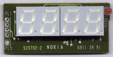
I've salvaged this module from a scrap Nokia Hotel TV, but it is fairly easy to build it yourself because it needs only a few components. The module can be controlled through the I²C bus, which makes it fairly easy to operate.
The Circuit Diagram

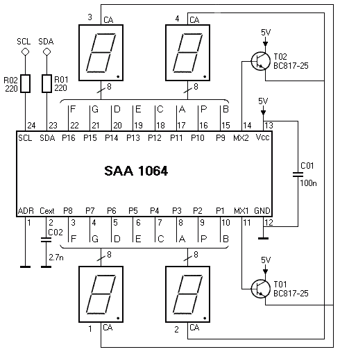
See, I told you it only uses a few components.
The heart of the circuit is of course the SAA1064, which is made by Philips.
It is operated in the so called dynamic mode, which means that the two 8-bit outputs of the chip can drive four 7-segment displays in a multiplexed mode.
We need two transistors to alternately switch between displays 1 and 3 or displays 2 and 4.
In my case the module is equipped with two SMD type transistors BC817-25, which can be substituted by any transistor with similar properties.
C01 is used to decouple the power lines.
And C02 is used in an oscillator which generates the multiplexing frequency.
You can measure a triangular shaped waveform of about 2.2V p-p @ 18kHz on pin 2 when the chip is operating in multiplexed mode.
This frequency is internally divided by 128 to produce the multiplex frequency of approximately 140Hz.
R01 and R02 are connected to the I²C bus.
By the way, you probably figured out already that the displays are of the Common Anode type.
That's all! Or is it? Not really, there's a little more to tell about this module I'm afraid. For starters the segment pin numbers are a little mixed up. Normally one would connect segment A to P1, segment B to P2, etc. For whatever reason Nokia didn't. Probably it was easier to route the PCB tracks from the chip to the displays this way. Fortunately they mixed up both channels in the same way, which makes it very simple to unscramble the lot in software. The table below shows the exact relation between the bit numbers and the segments:
| Bit # | Segment | Mask |
| 2 | A | 0000.0100 |
| 0 | B | 0000.0001 |
| 3 | C | 0000.1000 |
| 5 | D | 0010.0000 |
| 4 | E | 0001.0000 |
| 7 | F | 1000.0000 |
| 6 | G | 0100.0000 |
| 1 | DP | 0000.0010 |
A "1" in the mask means that the associated segment is on.
Addressing
Now we come to the point of addressing.
Every IC on the I²C bus requires a unique address.
Usually such ICs can select from a set of 2 to 8 possible addresses to allow multiple chips of the same type on one bus.
The SAA1064 can select from 4 different addresses by applying a specific voltage on pin 1 (ADR).
Unfortunately the address pin on my module is hard wired to ground.
Therefore changing the address of it requires some cutting and rewiring.
Fortunately that is only required when more than one module is to be used on the same I²C bus.

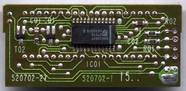
The track just above C02 (the small brown part in the upper right hand corner) is the track that connects the ADR pin of the SAA1064 to ground (right side of C02).
By cutting this track and connecting pin 1 of the SAA1064 directly to the Vcc you can simply select address $76 instead of $70.
Selecting any of the other address involves adding 2 resistors to create the appropriate voltage on pin 1.
A voltage of about 1.9V will select address $72, while a voltage of about 3.1V will select address $74.
The 4 little holes on the right hand side of the picture are the connections to the outside world. From top to bottom they are: SCL, SDA, GND and Vcc.
Communication

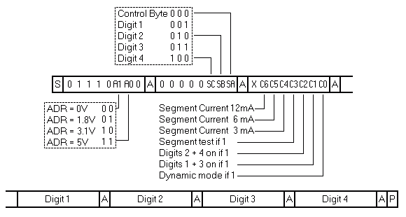
The diagram above shows a complete I²C message.
Such a message consists of an address byte and a total of 6 data bytes.
The diagram only shows a write message.
You can read from the device, but that will only tell you whether it was just powered up.
Thus not very useful, so I will restrict myself to the write mode only.
The address byte is mainly fixed, only 2 bits may differ depending on the voltage on the ADR pin.
On my module the ADR pin is hard wired to ground, which makes it respond to address $70.
The first data byte in the string is always a sub-address.
It selects what data byte is to be send next.
In most cases this sub-address byte is $00, which means that the next data byte is the control byte.
By using other sub-addresses you can skip right to the data byte you want to change.
In this example the sub-address must be $00 because we continue with sending the control byte next.
The control byte controls the behaviour of the chip.
It selects between static or dynamic mode, and whether the display(s) on both ports should be on or not.
It also allows you to switch on all segments in the segment test mode.
But most importantly it will allow you to control the segment current.
This is a nice property!
You may select a segment current from 3 to 21mA in steps of 3mA by setting the appropriate bits.
In my case the least significant bits have to be set, b3 must be cleared.
Bits 4 to 6 will set the display brightness.
The next 4 bytes are easily explained.
They are simply bit masks for each of the 4 digits of the module.
But remember, the segments on my module (and therefore the diagram at the beginning of this page) are mixed up a bit.
If you want to copy my projects that use this module without modification, you will also have to mix up the segments in the same way.
By the way: Did I mention that Display number 1 is the right most digit? I don't think I did. So I'd better tell you now. Display 1 is the right most digit, which means that the digits on the display are sent through the I²C bus in reverse order.
Note: For those of you who are not very familiar with the I²C bus, S means Start sequence, A means Acknowledge and P means Stop sequence.
